|
Nanotubes As They Are
NT-MDT provides the full range of modern SPM-based techniques for nanotubes visualizing and testing
Nanotubes are small enough so that only a few methods exist to visualize them. On the other hand they are the object of an extraordinary interest so that many modern scientific approaches are desirable to be applied to it. Probe
NanoLaboratory NTEGRA® provides a platform to successfully deal with nanotubes. Here are some nanotube images illustrating possibilities of different methods. They are presented as a gallery subdivided into four groups:
• SPM visualizing
• Electrical properties
• Chemical composition, spectral and optical properties
• Nanomanipulations
SPM is a Common Tool for Nanotubes Imaging
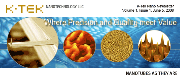
STM image of carbon nanotube deposted on HOPG substrate. Atomic structure of the nanotube is clearly visible.
Image courtesy of Prof. V.K. Nevolin, Moscow Institute of Electronic Enginerring, Russia. |
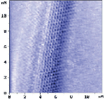 |
Carbon nanotubes on silicon surface. Phase imaging mode.
Sample courtesy of Dr. H.B. Chan, Department of Physics, University of Florida, USA. |
 |
STM (Scanning Tunneling Microscopy) allows viewing single nanotubes with atomic resolution. AFM (Atomic Force Microscopy) in turn provides much more contrasting modes and serves as a toolkit for testing large sets of physical properties along with visualization itself. Probe NanoLaboratory NTEGRA®Prima is a powerful and convenient SPM system. In most common cases it is the perfect choice for ultra-sensitive STM and high-accuracy AFM imaging.
Single Nanotube Spectral Characterization By Ultra-High Resolution Spectroscopy (TERS)
The mightiest system developed for advanced optical experiments is the NTEGRA®Spectra. In addition to most SPM methods available NTEGRA®Spectra provides the excellent performance in the following research areas:
1. Laser confocal microscopy (200 nm resolution in XY)
2. Raman micro-spectroscopy and Raman micro-imaging (200 nm resolution in XY)
3. Scanning near-field optical microscopy (SNOM, about 30 nm resolution in XY)
4. Single molecule detection, identification, and imaging on the base of local field enhancement effects (TERS,
SERS and enhanced fluorescence)
One more example of huge set of optical experiments available with the NTEGRA®Spectra is the visualization of
nanotube optical properties.
|
a — a specially prepared AFM probe (metal coated cantilever or etched metal wire) is precisely positioned inside a tightly focused laser spot.
b — intensity ofcarbon nanotube G- and D- Raman bands increases by several orders ofmagnitude when the special AFM probe is landed and positioned over a small (5 nm height) nanotube bundle - the effect of Tip enhanced Raman scattering (TERS).
c — "conventional" confocal Raman image of the nanotube bundle, the observed width of the bundle is ~250 nm (diffraction limit of confocal microscopy, laser wavelength - 633 nm).
d — TERS image of the same bundle - now the observed width is ~70 nm. Note, in this example, TERS provides more than 4-times better spatial resolution as compared to confocal microscopy. Resolution down to 10 nm and less is theoretically possible. Measurements are done with NTEGRA Spectra in Inverted configuration.
Data courtesy of Dr.S.Kharintsev, Dr.J.Loos, Dr.G.Hoffmann, Prof.G.de With, TUE, the Netherlands and Dr.P.Dorozhkin,NT-MDT Co. |
The mightiest system developed for advanced optical experiments is the NTEGRA®Spectra. In addition to most SPM methods available NTEGRA®Spectra provides the excellent performance in following research areas:
1. Laser confocal microscopy (200 nm resolution in XY)
2. Raman micro-spectroscopy and Raman micro-imaging (200 nm resolution in XY)
3. Scanning near-field optical microscopy (SNOM,about 30 nm resolution in XY)
4. Single molecule detection, identification, and imaging on the base of local field enhancement effects (TERS,
SERS and enhanced fluorescence)
One more example of huge set of optical experiments is available with the NTEGRA®Spectra is the visualization of
nanotube optical properties.
Long-Term Stability is the Base For Accurate Manipulations
 |
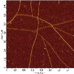
| The simplest example of nanomanipulations. Carbon nanotube shown on left image was pushed along specified direction (white arrow). Right image shows the nanotube in resulting position. Lines to move the probe along can be just drown by mouse. Otherwise templates of any complexity can easily be downloaded from graphics file. |
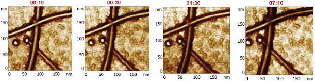 |
To assess the system long-term stability the same area of the sample with magnet particles coupled carbon nanotubes was imaged repetitively for a long time. Overall XY displacement of marker feature (e.g.magnet particle) for 7 hour was as small as about 35 nm.
Sample courtesy of Dr. H. B. Chan, Department of Physics, University of Florida, USA. |
There are three system characteristics that are crucial for success of nanomanipulations. All three are the most
profoundly developed within the NTEGRA®Therma Probe NanoLaboratory.
1. System stability. Exclusive design of both scanning and registration blocks (materials, geometry etc.) compensates most of temperature drifts - the main factor affecting both long-term stability and stability at changing temperature. Most of mechanical drifts are compensated due to the NTEGRA®platform design solutions.
2. Repeatability at high resolution. Repeatability means that one can zoom in for some details on large area, zoom out back getting the same large-scale image or simply rescan many times the same high resolution area. Integrated closed-loop operation sensors have the market-lowest noises providing perfect repeatability on any scanning areas down to 50 nm.
3. Convenient software. Extended nanolithography/manipulation package is pre-included into the Nova software. It allows most of the common nanomanipulations to be performed in a very convenient way through easy and intuitively clear interface. On the other hand the Nova PowerScript provides the maximum freedom in experiments of any complexity through macros making.
|
Electrical Characteristics Can Be Assayed by EFM and SKM
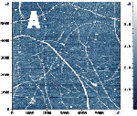

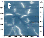
Mixture of carbon nanotubes of different thickness can be seen in topography (A), in electrostatic force microscopy (EFM, B), and
scanning Kelvin probe microscopy (SKM, C) modes. EFM shows that all nanotubes are charged. Differences in charge can be observed by SKM. The thickest nanotubes (diameter about 4 nm) show the lowest potential in SKM and the thinnest (diameter about
1.5 nm) have the highest potential (about 1.5 V).
Two-pass SPM methods like EFM SKM or MFM are very sensitive to the environment. In fact vacuum conditions can greatly improve the two-pass imaging quality increasing the cantilever's Q-factor. Probe NanoLaboratory NTEGRA®Aura provides much freedom to operate in low-vacuum conditions. In terms of atmosphere control, NTEGRA®Aura is the best-balanced solution because while the vacuum equipment is fitted to be very compact and economic it is still powerful. It takes only 1 minute to achieve 10-times Q-factor increase!
Nanowire as an Optical Fiber
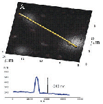
AFM of semiconductor nanowire (Mn-doped GaN) is shown on A. It has a diameter of about 300 nm as seen on a height profile crossing it
|

The nanowire shows fluorescence in near infrared when excited by a green laser (488 nm). Scanning laser confocal fluo-
rescence image of it is on C. D shows fluorescence images of the nanowire, being excited at its center by a tightly focused laser spot (~300 nm diameter). The nanowire is imaged by a cooled CCD camera in a "direct image" mode of the spectrograph; the excitation laser light is completely cut off by edge filters in this scheme (as well as in scanning laser confocal fluorescence detection scheme).
From the image (D) it is clear that the emission light is partially transmitted through the nanowire from the center to both ends.
|
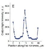
From light intensity profile (E) it can be determined that about 70% of emitted light is transmitted for more than 10µm.
Sample courtesy of Prof.Y.Bando, National Institute for Materials Science, Japan .
|
NTEGRA®Platform
Natural Integration of SPM to Non-SPM Methods and Easy Re-Specialization of Any Highly-Specialized System
NT-MDT has developed the NTEGRA®platform for joining the most powerful SPM facilities with the most modern and profound non-SPM scientific methods. As for SPM it can be run in low or high vacuum, with precise temperature control and unique thermo- and long-term stability. As for non-SPM facilities there is a high resolution optical observation available (down to 0.4 µm, HRV® option), Raman spectroscopy (NTEGRA®Spectra), tomography (NTEGRA®Tomo), electrochemistry methods and many more. The NTEGRA® concept key-point is that all facilities are naturally integrated within the whole system both on hardware and software levels. That is why re-specialization of any NTEGRA®
system into another one is very easy and economic.
With the Probe NanoLaboratory NTEGRA® your nanotubes experiments become not only more informative and accurate but also more pleasant! |